Description
This board FPGA based is the core of the system, it controls the logic analyzer, the scope, the arbitrary function generator, and the Frequencymeter
Summary
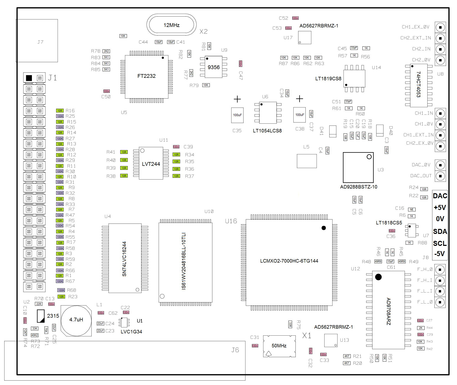
BLOCK DIAGRAM
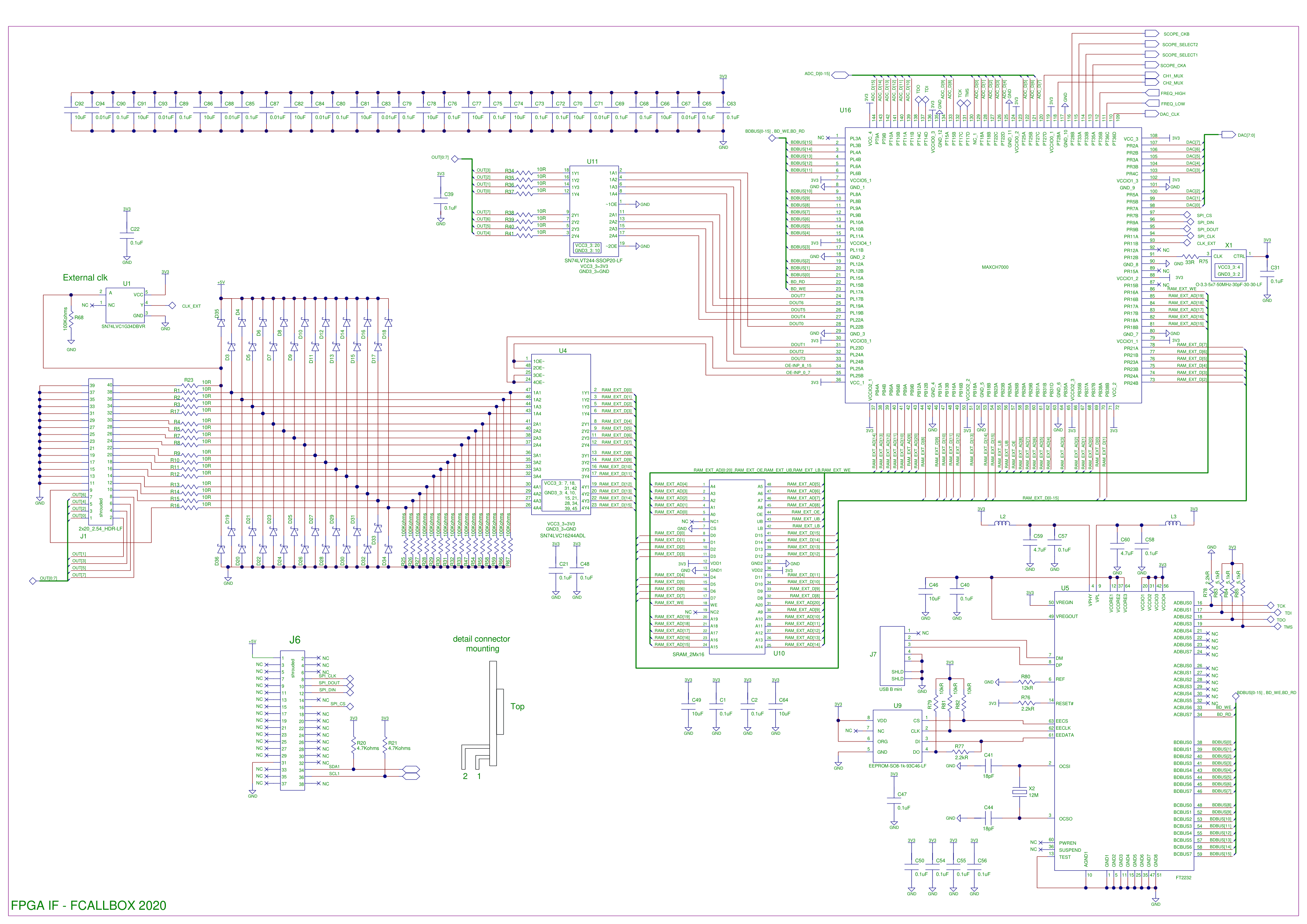
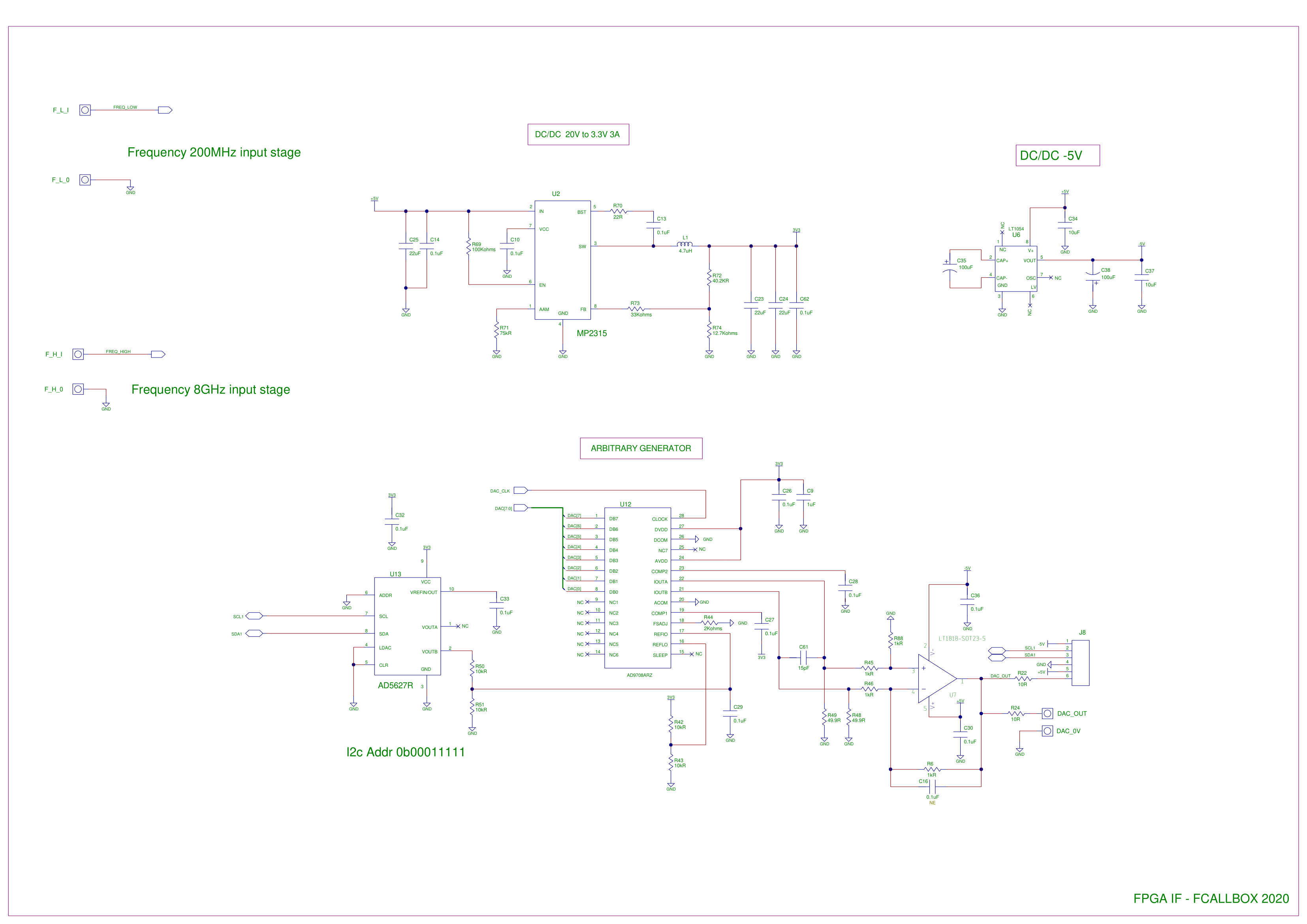
Schematic
Download the schematic here
Bill of material
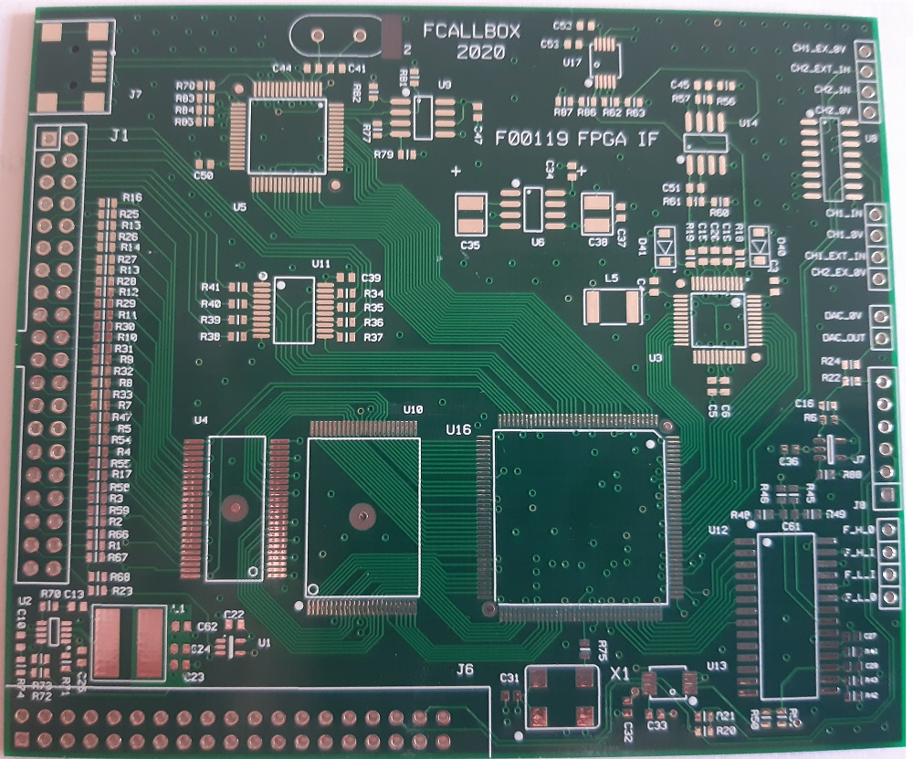
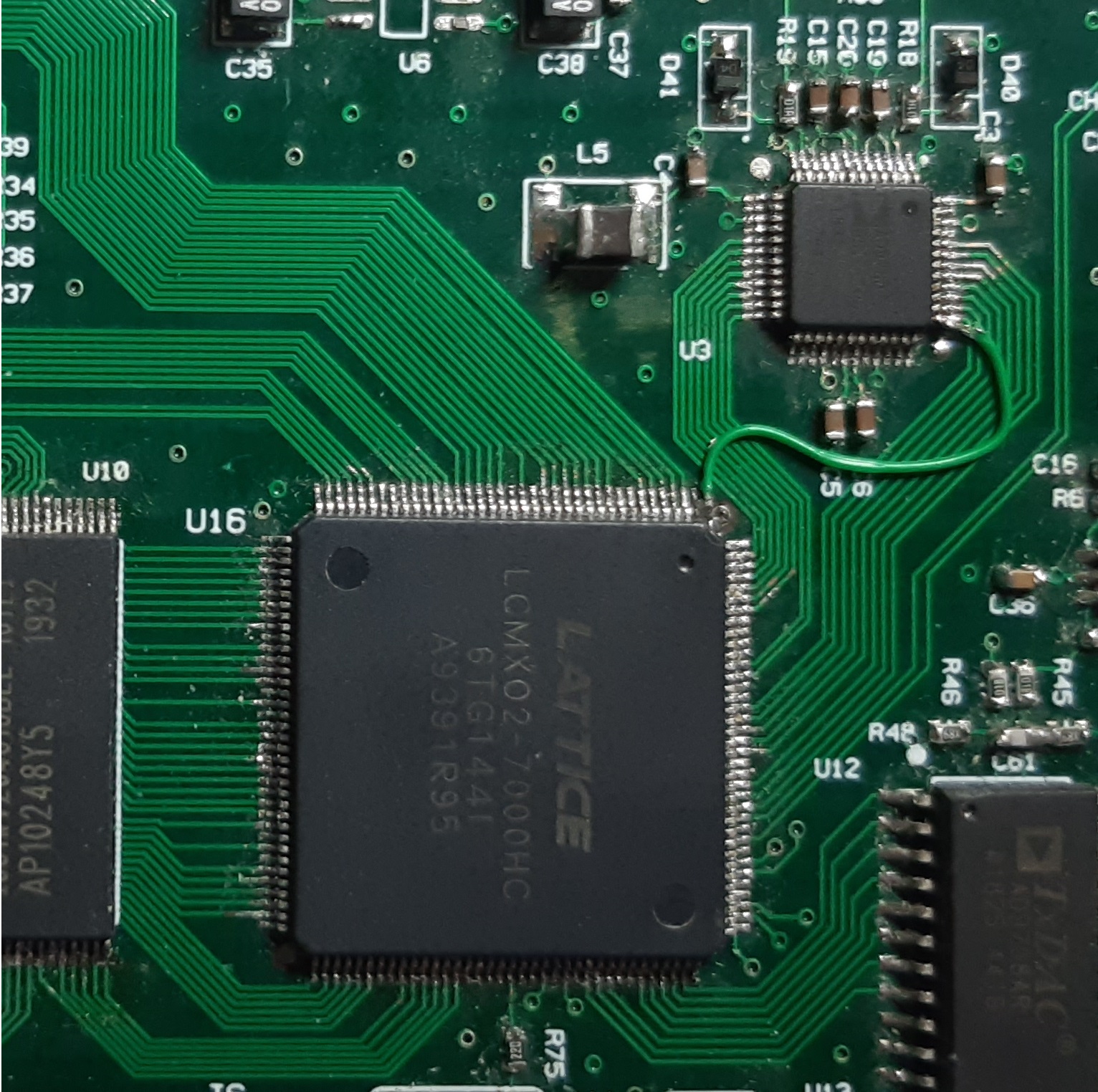
Top view
| Ref |
Description |
Vendor / reference |
Price |
| D40,D41 |
Diode schottky SDO323 BAS416 |
NXP |
2 x 0.16€ |
| R1,R2,R3,R4,R5,R7,R8,R9,R10,R11,R12,R13,R14,R15,R16,R17,R22,R23,R34,R35,R36,R37,R38,R39,R40,R41,R24 |
Resistor 10R 5% 0603 |
All brand |
28 x 0.02€ |
| R18,R19 |
Resistor 100R 5% 0603 |
All brand |
2 x 0.02€ |
| R25 à R33, R47,R54,R55,R58,R59,R66,R67,R68 |
Resistor 100KR 5% 0603 |
All brand |
17 x 0.02€ |
| R42,R86,R87,R62,R63,R79,R81,R82 |
Resistor 10K 1% 0603 |
All brand |
11 x 0.02€ |
| R48,R49 |
Resistor 49R9 1% 0603 |
All brand |
2 x 0.02€ |
| R50 |
Resistor 0R 1% 0603 |
All brand |
2 x 0.02€ |
| R45,R46 |
Resistor 1K 1% 0603 |
All brand |
8 x 0.02€ |
| R6,R88 |
Resistor 2K2 1% 0603 |
All brand |
8 x 0.02€ |
| R56,R60 |
Resistor 3K3 1% 0603 |
All brand |
8 x 0.02€ |
R57,R61 |
Resistor 5K6 1% 0603 |
All brand |
8 x 0.02€ |
| R73 |
Resistor 33K 1% 0603 |
All brand |
0.02€ |
| R75 |
Resistor 33R 1% 0603 |
All brand |
1 x 0.02€ |
| R70 |
Resistor 22R 1% 0603 |
All brand |
1 x 0.02€ |
| R20,R21 |
Resistor 4K7 1% 0603 |
All brand |
2 x 0.02€ |
| R44 |
Resistor 2K 1% 0603 |
All brand |
1 x 0.02€ |
| R77,R78 |
Resistor 2K2 1% 0603 |
All brand |
1 x 0.02€ |
| R72 |
Resistor 40K2 1% 0603 |
All brand |
1 x 0.02€ |
| R83,R84,R85 |
Resistor 5K1 1% 0603 |
All brand |
1 x 0.02€ |
| R74 |
Resistor 12K7 1% 0603 |
All brand |
1 x 0.02€ |
| R71 |
Resistor 68K 1% 0603 |
All brand |
1 x 0.02€ |
| C16 |
capacitor 10pF 50V 10% COG 0603 |
All brand |
1 x 0.05€ |
| C41,C44 |
capacitor 18pF 50V 10% COG 0603 |
All brand |
2 x 0.05€ |
| C45,C51 |
capacitor 33pF 50V 10% COG 0603 |
All brand |
2 x 0.05€ |
| C61 |
capacitor 15pF 50V 10% COG 0603 |
All brand |
0.05€ |
| C67 |
capacitor 10nF 50V 10% X5R 0603 |
All brand |
0.05€ |
| C20 |
capacitor 1uF 10V 10% X5R 0603 |
All brand |
0.05€ |
| C38 |
capacitor 100uF |
AVX F910J107MBAAJ6 All brand |
2 x 0.6€ |
| C10,C13,C22,C27,C29,C31,C32,C33,C36,C39,C47,C50,C53,C52,C62, |
capacitor 100nF 50V 10% X5R 0603 |
All brand |
31 x 0.03€ |
| C23,C24 |
capacitor 22uF 6.3V 10% X5R 0603 |
All brand |
2 x 0.3€ |
| C3,C4,C5,C6,C37,C34,C19,C15 |
capacitor 10uF 6.3V 10% X5R 0603 |
All brand |
8 x 0.06€ |
| L5 |
inductor 100uH 270mA 18120 |
EPCOS B82422A1223K10 or equivalent |
0.5€ |
| L1 |
inductor 47uH 6A 30mR 7x7 |
BOURNS SRP6540-4R7M or equivalent |
1 x 1€ |
| L2,L3 |
ferrite 600R 0603 |
TE BMB1J0600PN8 or equivalent |
2 x 0.1€ |
| U16 |
IC FPGA Machx02 7000HC TQFP144 |
Lattice LCMXO2-7000HC-6TG144 |
17.41€ |
| U9 |
IC EEPROM 93LC56 SO8 |
Microchip 93LC56BT-I/SN or equivalent |
0.2€ |
| U5 |
IC FT2232HL LQFP 64 |
Microchip FT2232HL |
6€ |
| U1 |
IC SN74LVC1G34DBVR single buffer gate |
TI SN74LVC1G34DBVR or equivalent |
0.24€ |
| U11 |
IC SN74LVT244 SSOP20 |
Texas Instruments SN74LVT244BDBR |
0.7€ |
| U4 |
IC SN74LVC16244 buffer 16 inputs SSOP48 |
Texas Instruments SN74LVC16244ADL |
1.1€ |
| U12 |
IC DAC 8 bits 100Mbps |
Analog Devices AD9708ARZ |
6.5€ |
| U13,U17 |
IC DAC AD5627R 12its SOIC-8 |
Analog Devices AD5627RBRMZ-1 |
2 x 4€ |
| U3 |
IC ADC dual 8 bits 100Mbps |
Analog Devices AD9288BSTZ-10 |
19.4€ |
| U14 |
IC LT1819 AOP 400MHz double SO8 |
Analog Devices LT1819CS8#TRPBF |
2.3€ |
| U2 |
IC MP2315 SOT23-8 |
MPS (Monolithic Power System) / MP2315GJ |
2€ |
| U7 |
IC LT1818 AOP 400MHz single SOT23-5 |
Analog Devices LT1818CS5#TRMPBF |
1.44€ |
| U8 |
IC 74HCT4053D SOIC16 |
Texas Instruments 74HCT4053D |
0.4€ |
| U10 |
SRAM 10ns 2Mx16 TSOP48 12x20mm 0.5mm |
ISSI IS61WV204816BLL-10TLI |
19.6€ |
| X1 |
oscillator 50MHz 50ppm 5x7 |
CTS CB3LV-3C-50M0000 or equivalent |
1.2€ |
| X2 |
xtal 12MHz (AT, 16pF) 30ppm HC49U |
Abracon ABL-8.912MHz-B4Y or equivalent |
0.3€ |
| J1 |
connector HE10 2x20 2.54mm |
TE 6-103166-8 |
8€ |
| J6 |
Connector male right angle 2x19 pitch 2.54mm |
All brand |
1€ |
| J8 |
Connector male 1x6 pitch 2.54mm |
All brand |
1€ |
| J7 |
USB mini B type jack horizontal SMD |
CUI UJ2-MBH-1-SMT-TR |
0.43€ |
|
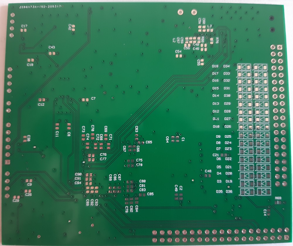
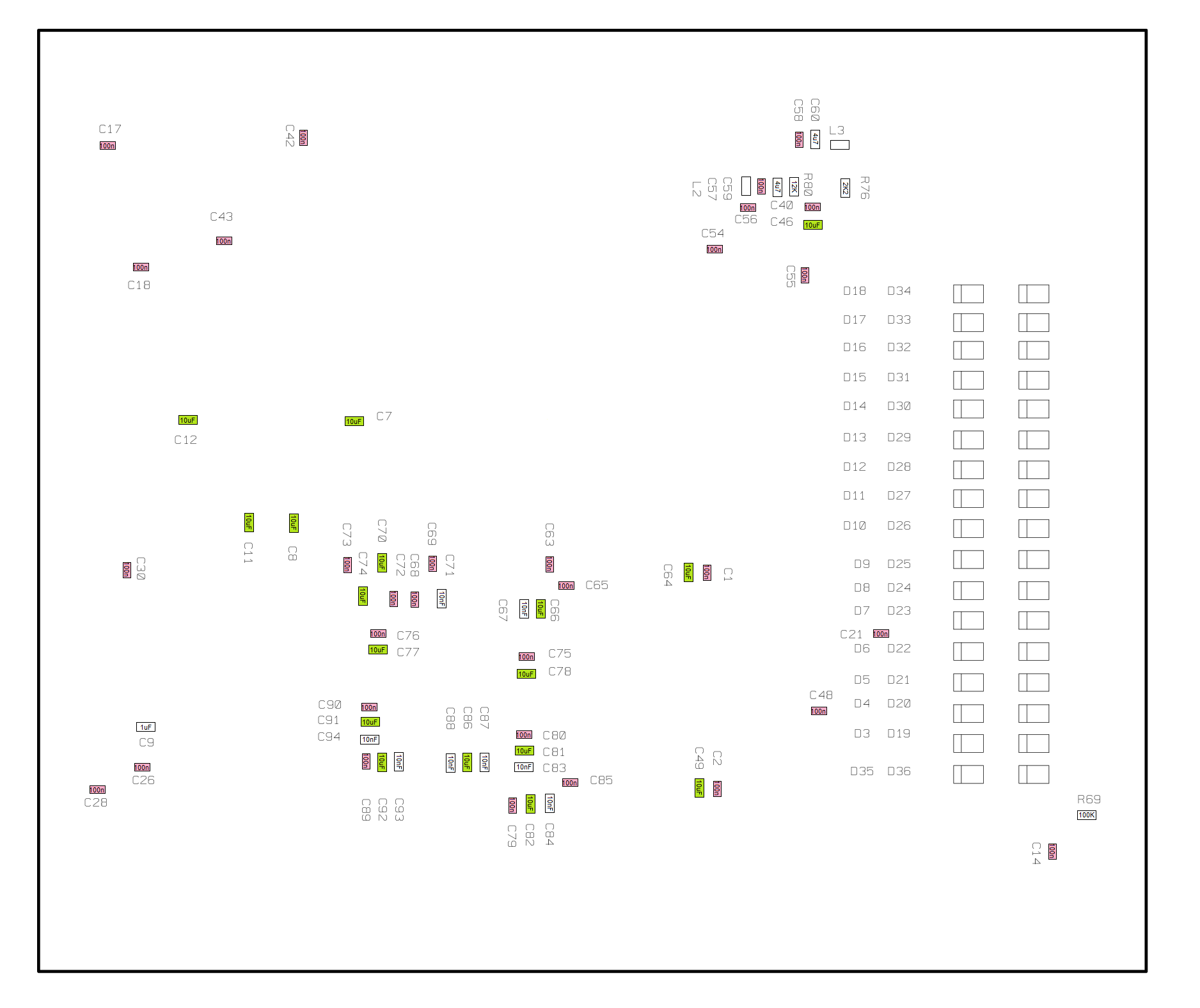
Bottom view
| Ref |
Description |
Vendor / reference |
Prix |
| D3 à D36 |
Diode schottky SDO323 BAS416 |
NXP |
34 x 0.16€ |
| R69 |
Resistor 100KR 5% 0603 |
All brand |
1 x 0.02€ |
| R76 |
Resistor 2K2 1% 0603 |
All brand |
1 x 0.02€ |
| R80 |
Resistor 12K 1% 0603 |
All brand |
1 x 0.02€ |
| C1,C2,C14,C17,C18,C21,C40,C42,C43,C48,C54,C55,C56,C57,C58,C63,C65,C68,C69,C72,C73,C75,C76,C79,C80,C85,C89,C90,C26,C28,C30 |
capacitor 100nF 50V 10% X5R 0603 |
All brand |
31 x 0.03€ |
| C71,C83,C84,C87,C88,C93,C94, |
capacitor 10nF 50V 10% X5R 0603 |
All brand |
7 x 0.03€ |
| C9 |
capacitor 1uF 10V 10% X5R 0603 |
All brand |
1 x 0.05€ |
| C59,C60 |
capacitor 4.7uF 50V 10% X5R 0603 |
All brand |
2 x 0.05€ |
| C7,C8,C11,C12,C46,C49,C64,C66,C70,C74,C77,C78,C81,C82,C86,C91,C92 |
capacitor 10uF 6.3V 10% X5R 0603 |
All brand |
17 x 0.06€ |
| C25 |
capacitor 22uF 6.3V 10% X5R 0603 |
All brand |
1 x 0.3€ |
|
Estimated cost in 2021 (Mouser) : around € HT
PCB
The PCB F00119 is 100x85mm .
Download here the PCB manucfacturing files
Board assembly
|
Top view
|
Download the top view assy (in pdf format, for component search location)
Download the top view assy with component value
|
Bottom view
|
Download the top view assy (in pdf format, for component search location)
Download the top view assy with component value
Modifications :
To reduce the noise on the scope channels, solde 4 x 49R9 on inputs : CH1_EX_0V & CH2_EXT_IN , CH2_IN & CH2_0V , CH1_IN & CH1_0V , CH1_EXT_IN & CH2_EX_0V
|
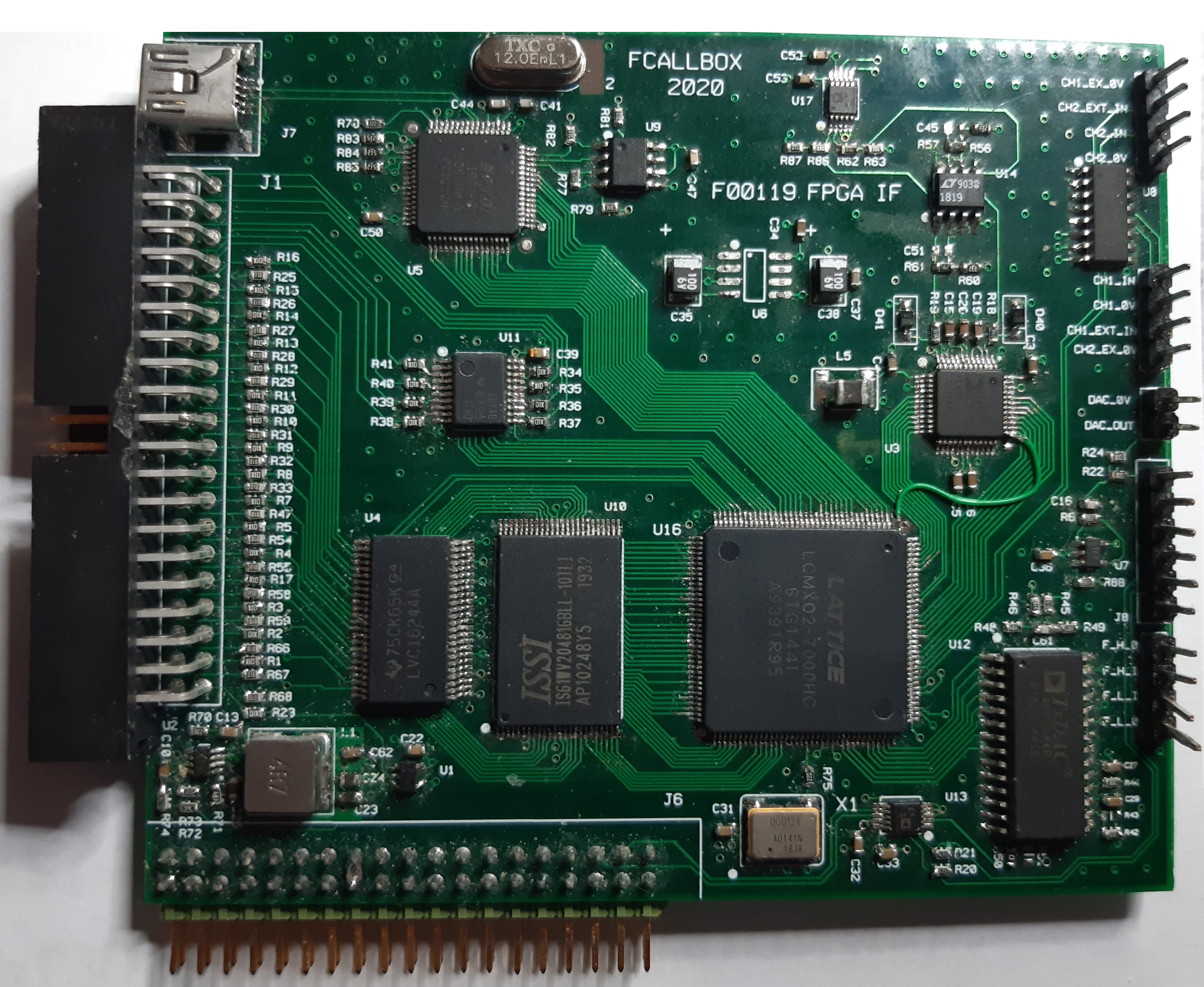
Picture of the PCB
|
FPGA FTDI E2P programmation
To get the FTDI interfacing the FPGA identified by the Raspberry, a serial number must be written into the E2P.
Program the serial number FT2024 with FT_PROG

FPGA CODE IMPLEMENTATION
REGISTERS :
| REGISTERS WRITABLE SUMMARY |
| Addr | function name | description |
|---|
| 01 | FPGA_REG_LOGIC_DOUT | Write 8bits on the DOUT outputs |
| 02 | FPGA_REG_LOGIC_DIN_GPIO | set GPIO for 16 logic inputs selection |
| 03 | FPGA_REG_SCOPE_GPIO | set GPIO for scope pins selection |
| 04 | FPGA_REG_FR_LG_SAMPLING | set frequency sampling for Frequency meter and Logic Analyser and misc bits |
| 05 | FPGA_REG_WRITE_RAM_DATA | set 16bits data to write in RAM LOGIC Analyzer / SCOPE or 8 bits data for LOGIC DOUT or DDS RAM |
| 06 | FPGA_REG_WRITE_RAM_REG | bits register for LOGIC Analyzer / SCOPE and LOGIC DOUT or DDS |
| 07 | FPGA_REG_ANAL_TRIG_DONT_CARE | LOGIC Analyzer trigger : don't care bits |
| 08 | FPGA_REG_ANAL_TRIG_EDG_UP | LOGIC Analyzer trigger : Edge UP bits |
| 09 | FPGA_REG_ANAL_TRIG_EDG_DW | LOGIC Analyzer trigger : Edge DOWN bits |
| 10 | FPGA_REG_ANAL_TRIG_LV0 | LOGIC Analyzer trigger : LEVEL 0 bits |
| 11 | FPGA_REG_ANAL_TRIG_LV1 | LOGIC Analyzer trigger : LEVEL 1 bits |
| 12 | FPGA_REG_DDS_CLK_MSB | set frequency sampling for LOGIC DOUT or DDS |
| 13 | FPGA_REG_DDS_CLK_LSB | set frequency sampling for LOGIC DOUT or DDS |
| 14 | FPGA_REG_DDS_SIZE | set Arbitrary Generator pattern size |
| 15 | FPGA_SCOPE_TRIGGER_THRESHOLD | set Scope trigger thresholds |
| 16 | FPGA_SCOPE_TIME_BASE | set Scope time base |
| 17 | FPGA_SCOPE_SETTING | set Scope settings |
| 18 | FPGA_SCOPE_PULSE_MSB | set Scope trigger pulse time MSB |
| 19 | FPGA_SCOPE_PULSE_LSB | set Scope trigger pulse time LSB |
| REGISTERS READABLE SUMMARY |
| Addr | function name | description |
|---|
| 01 | FPGA_REG_RAM_ADDR_READ | read current RAM address |
| 02 | FPGA_REG_RAM_DATA_READ | read current RAM data |
| 03 | FPGA_REG_FREQ_LSB_READ | read Frequency from frequeny meter LSB (D0-D15) |
| 04 | FPGA_REG_FREQ_MSB_READ | read Frequency from frequeny meter MSB (D8-D31) |
| 05 | FPGA_REG_STATUS | read FPGA status bits |
REGISTERS WRITABLE :
| Register 01 : FPGA_REG_LOGIC_DOUT |
Write 8bits on the DOUT outputs
SPI format <0x0001 > <Dout> :
| A15 | A14 | A13 | A12 | A11 | A10 | A09 | A08 | A07 | A06 | A05 | A04 | A03 | A02 | A01 | A00 |
|---|
| 0 | 0 | 0 | 0 | 0 | 0 | 0 | 0 | 0 | 0 | 0 | 0 | 0 | 0 | 0 | 1 |
| D15 | D14 | D13 | D12 | D11 | D10 | D09 | D08 | D07 | D06 | D05 | D04 | D03 | D02 | D01 | D00 |
|---|
| - | - | - | - | - | - | - | - | D07 | D06 | D05 | D04 | D03 | D02 | D01 | D00 |
| Register 02 : FPGA_REG_LOGIC_DIN_GPIO |
set GPIO for 16 logic inputs selection
SPI format <0x0002 > <bits> :
| A15 | A14 | A13 | A12 | A11 | A10 | A09 | A08 | A07 | A06 | A05 | A04 | A03 | A02 | A01 | A00 |
|---|
| 0 | 0 | 0 | 0 | 0 | 0 | 0 | 0 | 0 | 0 | 0 | 0 | 0 | 0 | 1 | 0 |
| D15 | D14 | D13 | D12 | D11 | D10 | D09 | D08 | D07 | D06 | D05 | D04 | D03 | D02 | D01 | D00 |
|---|
| - | - | - | - | - | - | - | - | - | - | - | - | - | OE INO 8_15 | OE INO 0_7 | OE INP DBL |
D0 : OE INP DBL : select buffer to put inputs 0 to 7 on RAM data bus 8 to 15 , default 0 (not selected)
D1 : OE INO 0_7 : select buffer to put inputs 0 to 7 on RAM data bus 0 to 7 , default 0 (not selected)
D2 : OE INP DBL : select buffer to put inputs 8 to 15 on RAM data bus 8 to 15 , default 0 (not selected)
| Register 03 : FPGA_REG_SCOPE_GPIO |
set GPIO for scope pins selection
SPI format <0x0003 > <bits> :
| A15 | A14 | A13 | A12 | A11 | A10 | A09 | A08 | A07 | A06 | A05 | A04 | A03 | A02 | A01 | A00 |
|---|
| 0 | 0 | 0 | 0 | 0 | 0 | 0 | 0 | 0 | 0 | 0 | 0 | 0 | 0 | 1 | 1 |
| D15 | D14 | D13 | D12 | D11 | D10 | D09 | D08 | D07 | D06 | D05 | D04 | D03 | D02 | D01 | D00 |
|---|
| - | - | - | - | - | - | - | - | - | - | CH2 MUX | CH1 MUX | D04 | D03 | SCOPE SELECT2 | SCOPE SELECT1 |
D0 : SCOPE SELECT1 : , default 0 (not selected)
D1 : SCOPE SELECT2 : , default 0 (not selected)
D2 :
D3 :
D4 : CH1 MUX : , default 0 (CH1 internal input selected)
D5 : CH2 MUX : , default 0 (CH2 internal input selected)
| Register 04 : FPGA_REG_FR_LG_SAMPLING |
set frequency sampling for Frequency meter and Logic Analyser
SPI format <0x0004 > <bits> :
| A15 | A14 | A13 | A12 | A11 | A10 | A09 | A08 | A07 | A06 | A05 | A04 | A03 | A02 | A01 | A00 |
|---|
| 0 | 0 | 0 | 0 | 0 | 0 | 0 | 0 | 0 | 0 | 0 | 0 | 0 | 1 | 0 | 0 |
| D15 | D14 | D13 | D12 | D11 | D10 | D09 | D08 | D07 | D06 | D05 | D04 | D03 | D02 | D01 | D00 |
|---|
| FR/PE | FR_START | FR_DTY | FR_FREQ_MOD | FR_FREQ_COUNT | FR_FREQ_CLR | FR_DIV1 | FR_DIV0 | FR_INP1 | FR_INP0 | CNT_INP | - | LG_DIV3 | LG_DIV2 | LG_DIV1 | LG_DIV0 |
D15 : FR/PE : Frequency (1) or Period (0) measurement mode
D14 : FR_START : Frequency or Period measurement start, actif at 1, must be reset manually by setting bit to 0
D13 : FR_DTY : Duty Cycle measurement, actif at 1, measure TON, must be used with periode measurement to compute the duty cycle
D12 : FR_FREQ_MOD : Frequency or counter mode, Frequency at 1
D11 : FR_FREQ_COUNT : counter mode, counting input pulses when 1
D10 : FR_FREQ_CLR : counter mode, reset counter when 1
D09-D08 : FR_DIV1-0 : Frequency Meter gate : 10ms (0) , 100ms (1) , 1s (2) , 10s (3)
D07-D06 : FR_INP1-0 : Frequency Meter input selection : Freq low (0) , Freq Hig (1) , Freq SCOPE (2)
D05 : CNT_INP : Counter START/STOP input selection : CLK_EXT input (0) , button on screen (1)
D03-D00 : LG_DIV3-0 : Logic Analyser sampling :
100MHz (0),50MHz (1) , 25MHz (2), 10MHz (3), 5MHz (4) , 2.5MHz (5), 1MHz (6), ,500KHz (7) , 250KHz (8), 100KHz (9),
50KHz (10) , 25KHz (11), 10KHz (12), 5KHz (13) , 2.5KHz (14), 1KHz (15),
| Register 05 : FPGA_REG_WRITE_RAM_DATA |
set 16bits data to write in RAM LOGIC Analyzer / SCOPE or 8 bits data for LOGIC DOUT or DDS RAM
SPI format <0x0005 > <bits> :
| A15 | A14 | A13 | A12 | A11 | A10 | A09 | A08 | A07 | A06 | A05 | A04 | A03 | A02 | A01 | A00 |
|---|
| 0 | 0 | 0 | 0 | 0 | 0 | 0 | 0 | 0 | 0 | 0 | 0 | 0 | 1 | 0 | 1 |
| D15 | D14 | D13 | D12 | D11 | D10 | D09 | D08 | D07 | D06 | D05 | D04 | D03 | D02 | D01 | D00 |
|---|
| D15 | D14 | D13 | D12 | D11 | D10 | D09 | D08 | D07 | D06 | D05 | D04 | D03 | D02 | D01 | D00 |
D15 - D00 : data for RAM LOGIC Analyzer/ SCOPE or 8 bits data for LOGIC DOUT or DDS RAM
| Register 06 : FPGA_REG_WRITE_RAM_REG |
bits register for LOGIC Analyzer / SCOPE and LOGIC DOUT or DDS
SPI format <0x0006 > <bits> :
| A15 | A14 | A13 | A12 | A11 | A10 | A09 | A08 | A07 | A06 | A05 | A04 | A03 | A02 | A01 | A00 |
|---|
| 0 | 0 | 0 | 0 | 0 | 0 | 0 | 0 | 0 | 0 | 0 | 0 | 0 | 1 | 1 | 0 |
| D15 | D14 | D13 | D12 | D11 | D10 | D09 | D08 |
|---|
| LG_SCP_CNT_CLR | LG_SCP_CNT_PROG_MOD | LG_SCP_CNT_INC | LG_SCP_RAM_WE | D11 | D10 | D09 | D08 |
| D07 | D06 | D05 | D04 | D03 | D02 | D01 | D00 |
|---|
| D07 | DOUT_DDS_DIS_CLR | DOUT_DDS_ONE_SHOT | DOUT_DDS_CNT_CLR | DOUT_DDS_CNT_PROG_MOD | DOUT_DDS_CNT_INC | DOUT_DDS_RAM_WE | RAM_DIN_WRITE_or_INPUT |
D15 LG_SCP_CNT_CLR : reset counter RAM Analyzer/SCOPE (actif at 1)
D14 LG_SCP_CNT_PROG_MOD : set Analyzer/SCOPE in RUN mode when 0 and RAM write or read mode when set to 1 (note in PROG mode the triggers are reseted)
D13 LG_SCP_CNT_INC : clock counter RAM Analyzer/SCOPE (used in RAM write or read mode)
D12 LG_SCP_RAM_WE : Write RAM Analyzer/SCOPE (at 1 to set the WRITE mode and 0 for read)
D06 DOUT_DDS_DIS_CLR :
D05 DOUT_DDS_ONE_SHOT :
D04 DOUT_DDS_CNT_CLR : reset counter LOGIC DOUT or DDS (actif at 1)
D03 DOUT_DDS_CNT_PROG_MOD : set LOGIC DOUT or DDS in RUN mode when 0 and RAM write or run mode when set to 1
D02 DOUT_DDS_CNT_INC : clock counter LOGIC DOUT or DDS (used in RAM write or run mode)
D01 DOUT_DDS_RAM_WE : Write LOGIC DOUT or DDS (at 1 to set the WRITE mode and 0 for run mode)
D00 RAM_DIN_WRITE_or_INPUT : at 1 to set the value of FPGA_REG_WRITE_RAM_DATA register on data in of the 2 RAMs , at 0 to present the LOGIC inputs 0-15
| Register 07 : FPGA_REG_ANAL_TRIG_DONT_CARE |
LOGIC Analyzer trigger : don't care bits
SPI format <0x0007 > <bits> :
| A15 | A14 | A13 | A12 | A11 | A10 | A09 | A08 | A07 | A06 | A05 | A04 | A03 | A02 | A01 | A00 |
|---|
| 0 | 0 | 0 | 0 | 0 | 0 | 0 | 0 | 0 | 0 | 0 | 0 | 0 | 1 | 1 | 1 |
| D15 | D14 | D13 | D12 | D11 | D10 | D09 | D08 | D07 | D06 | D05 | D04 | D03 | D02 | D01 | D00 |
|---|
| D15 | D14 | D13 | D12 | D11 | D10 | D09 | D08 | D07 | D06 | D05 | D04 | D03 | D02 | D01 | D00 |
set bit to 1 to define input bit trigger to Don't care, the trigger will not take care of any event on the pin to 1 (D15-D0 correspond to inputs 16-1)
| Register 08 : FPGA_REG_ANAL_TRIG_EDG_UP |
LOGIC Analyzer trigger : Edge UP bits
SPI format <0x0008 > <bits> :
| A15 | A14 | A13 | A12 | A11 | A10 | A09 | A08 | A07 | A06 | A05 | A04 | A03 | A02 | A01 | A00 |
|---|
| 0 | 0 | 0 | 0 | 0 | 0 | 0 | 0 | 0 | 0 | 0 | 0 | 1 | 0 | 0 | 0 |
| D15 | D14 | D13 | D12 | D11 | D10 | D09 | D08 | D07 | D06 | D05 | D04 | D03 | D02 | D01 | D00 |
|---|
| D15 | D14 | D13 | D12 | D11 | D10 | D09 | D08 | D07 | D06 | D05 | D04 | D03 | D02 | D01 | D00 |
set bit to 1 to define input bit trigger as edge rising event (D15-D0 correspond to inputs 16-1)
| Register 09 : FPGA_REG_ANAL_TRIG_EDG_DW |
LOGIC Analyzer trigger : Edge DOWN bits
SPI format <0x0009 > <bits> :
| A15 | A14 | A13 | A12 | A11 | A10 | A09 | A08 | A07 | A06 | A05 | A04 | A03 | A02 | A01 | A00 |
|---|
| 0 | 0 | 0 | 0 | 0 | 0 | 0 | 0 | 0 | 0 | 0 | 0 | 1 | 0 | 0 | 1 |
| D15 | D14 | D13 | D12 | D11 | D10 | D09 | D08 | D07 | D06 | D05 | D04 | D03 | D02 | D01 | D00 |
|---|
| D15 | D14 | D13 | D12 | D11 | D10 | D09 | D08 | D07 | D06 | D05 | D04 | D03 | D02 | D01 | D00 |
set bit to 1 to define input bit trigger as edge falling event (D15-D0 correspond to inputs 16-1)
| Register 10 : FPGA_REG_ANAL_TRIG_LV0 |
LOGIC Analyzer trigger : LEVEL 0 bits
SPI format <0x000a > <bits> :
| A15 | A14 | A13 | A12 | A11 | A10 | A09 | A08 | A07 | A06 | A05 | A04 | A03 | A02 | A01 | A00 |
|---|
| 0 | 0 | 0 | 0 | 0 | 0 | 0 | 0 | 0 | 0 | 0 | 0 | 1 | 0 | 1 | 0 |
| D15 | D14 | D13 | D12 | D11 | D10 | D09 | D08 | D07 | D06 | D05 | D04 | D03 | D02 | D01 | D00 |
|---|
| D15 | D14 | D13 | D12 | D11 | D10 | D09 | D08 | D07 | D06 | D05 | D04 | D03 | D02 | D01 | D00 |
set bit to 1 to define input bit trigger as ZERO level state (D15-D0 correspond to inputs 16-1)
| Register 11 : FPGA_REG_ANAL_TRIG_LV1 |
LOGIC Analyzer trigger : LEVEL 1 bits
SPI format <0x000b > <bits> :
| A15 | A14 | A13 | A12 | A11 | A10 | A09 | A08 | A07 | A06 | A05 | A04 | A03 | A02 | A01 | A00 |
|---|
| 0 | 0 | 0 | 0 | 0 | 0 | 0 | 0 | 0 | 0 | 0 | 0 | 1 | 0 | 1 | 1 |
| D15 | D14 | D13 | D12 | D11 | D10 | D09 | D08 | D07 | D06 | D05 | D04 | D03 | D02 | D01 | D00 |
|---|
| D15 | D14 | D13 | D12 | D11 | D10 | D09 | D08 | D07 | D06 | D05 | D04 | D03 | D02 | D01 | D00 |
set bit to 1 to define input bit trigger as ONE level state (D15-D0 correspond to inputs 16-1)
| Register 12 : FPGA_REG_DDS_CLK_MSB |
set frequency sampling for LOGIC DOUT or DDS
SPI format <0x000c > <bits> :
| A15 | A14 | A13 | A12 | A11 | A10 | A09 | A08 | A07 | A06 | A05 | A04 | A03 | A02 | A01 | A00 |
|---|
| 0 | 0 | 0 | 0 | 0 | 0 | 0 | 0 | 0 | 0 | 0 | 0 | 1 | 1 | 0 | 0 |
| D15 | D14 | D13 | D12 | D11 | D10 | D09 | D08 | D07 | D06 | D05 | D04 | D03 | D02 | D01 | D00 |
|---|
| D15 | D14 | D13 | D12 | D11 | D10 | D09 | D08 | D07 | D06 | D05 | D04 | DDS_DIV3 | DDS_DIV2 | DDS_DIV1 | DDS_DIV0 |
D15-D00 : LOGIC DOUT or DDS sampling MSB
| Register 13 : FPGA_REG_DDS_CLK_LSB |
set frequency sampling for LOGIC DOUT or DDS
DDS sampling = 100MHz / 2 / val (31bits) , if val =0 then sampling = 100MHz
SPI format <0x000d > <bits> :
| A15 | A14 | A13 | A12 | A11 | A10 | A09 | A08 | A07 | A06 | A05 | A04 | A03 | A02 | A01 | A00 |
|---|
| 0 | 0 | 0 | 0 | 0 | 0 | 0 | 0 | 0 | 0 | 0 | 0 | 1 | 1 | 0 | 1 |
| D15 | D14 | D13 | D12 | D11 | D10 | D09 | D08 | D07 | D06 | D05 | D04 | D03 | D02 | D01 | D00 |
|---|
| D15 | D14 | D13 | D12 | D11 | D10 | D09 | D08 | D07 | D06 | D05 | D04 | DDS_DIV3 | DDS_DIV2 | DDS_DIV1 | DDS_DIV0 |
D15-D00 : LOGIC DOUT or DDS sampling LSB
| Register 14 : FPGA_REG_DDS_SIZE |
set Arbitrary Generator pattern size
SPI format <0x000e > <bits> :
| A15 | A14 | A13 | A12 | A11 | A10 | A09 | A08 | A07 | A06 | A05 | A04 | A03 | A02 | A01 | A00 |
|---|
| 0 | 0 | 0 | 0 | 0 | 0 | 0 | 0 | 0 | 0 | 0 | 0 | 1 | 1 | 1 | 0 |
| D15 | D14 | D13 | D12 | D11 | D10 | D09 | D08 | D07 | D06 | D05 | D04 | D03 | D02 | D01 | D00 |
|---|
| - | - | - | - | - | - | D09 | D08 | D07 | D06 | D05 | D04 | D03 | D02 | D01 | D0 |
D09-D00 : pattern size 0 to 1023
| Register 15 : FPGA_SCOPE_TRIGGER_THRESHOLD |
set Scope trigger thresholds
SPI format <0x000f > <bits> :
| A15 | A14 | A13 | A12 | A11 | A10 | A09 | A08 | A07 | A06 | A05 | A04 | A03 | A02 | A01 | A00 |
|---|
| 0 | 0 | 0 | 0 | 0 | 0 | 0 | 0 | 0 | 0 | 0 | 0 | 1 | 1 | 1 | 1 |
| D15 | D14 | D13 | D12 | D11 | D10 | D09 | D08 | D07 | D06 | D05 | D04 | D03 | D02 | D01 | D00 |
|---|
| D15 | D14 | D13 | D12 | D11 | D10 | D09 | D08 | D07 | D06 | D05 | D04 | D03 | D02 | D01 | D0 |
D15-D08 : Threshold high
D07-D00 : Threshold low
| Register 16 : FPGA_SCOPE_TIME_BASE |
set Scope time base
SPI format <0x0010 > <bits> :
| A15 | A14 | A13 | A12 | A11 | A10 | A09 | A08 | A07 | A06 | A05 | A04 | A03 | A02 | A01 | A00 |
|---|
| 0 | 0 | 0 | 0 | 0 | 0 | 0 | 0 | 0 | 0 | 0 | 1 | 0 | 0 | 0 | 0 |
| D15 | D14 | D13 | D12 | D11 | D10 | D09 | D08 | D07 | D06 | D05 | D04 | D03 | D02 | D01 | D00 |
|---|
| D15 | D14 | D13 | D12 | D11 | D10 | D09 | D08 | D07 | D06 | D05 | D04 | D03 | D02 | D01 | D0 |
D04-D00 : time base :
250ns (0),500ns (1) , 1us (2), 2.5us (3), 5us (4) , 10us (5), 25us (6), ,50us (7) , 100us (8), 250us (9) , 500us (10) , 1ms (11) , 2.5ms (12)
5ms (13), 10ms (14), 25ms (15), 50ms (16) , 100ms (17) , 250ms (18) , 500ms (19) , 1s (20) , 2.5s (21) , 5s (22) , 10s (23) , 25s (24) , 50s (25) , EXT (26)
| Register 17 : FPGA_SCOPE_SETTING |
set Scope settings
SPI format <0x0011 > <bits> :
| A15 | A14 | A13 | A12 | A11 | A10 | A09 | A08 | A07 | A06 | A05 | A04 | A03 | A02 | A01 | A00 |
|---|
| 0 | 0 | 0 | 0 | 0 | 0 | 0 | 0 | 0 | 0 | 0 | 1 | 0 | 0 | 0 | 1 |
| D15 | D14 | D13 | D12 | D11 | D10 | D09 | D08 | D07 | D06 | D05 | D04 | D03 | D02 | D01 | D00 |
|---|
| D15 | D14 | D13 | D12 | D11 | D10 | D09 | D08 | D07 | D06 | D05 | TR_PUL_S | TR_TYP1 | TR_TYP2 | TR_SRC1 | TR_SRC0 |
D04 TR_PUL_S : trigger pulse sign, 0 pulse must be < time pulse , 1 pulse must be > time pulse
D03-D02 TR_TYP1-TR_TYP0 : Trigger Type : Edge rise (00) Edge fall(01) Pulse positive(10) Pulse negative (11)
D01-D00 TR_SRC1-TR_SRC0: Trigger source : CH1 (00) CH2 (01) EXT (10)
| Register 18 : FPGA_SCOPE_PULSE_MSB |
set Scope trigger pulse time MSB
SPI format <0x0012 > <bits> :
| A15 | A14 | A13 | A12 | A11 | A10 | A09 | A08 | A07 | A06 | A05 | A04 | A03 | A02 | A01 | A00 |
|---|
| 0 | 0 | 0 | 0 | 0 | 0 | 0 | 0 | 0 | 0 | 0 | 1 | 0 | 0 | 1 | 0 |
| D15 | D14 | D13 | D12 | D11 | D10 | D09 | D08 | D07 | D06 | D05 | D04 | D03 | D02 | D01 | D00 |
|---|
| D15 | D14 | D13 | D12 | D11 | D10 | D09 | D08 | D07 | D06 | D05 | D04 | D03 | D02 | D01 | D00 |
D15-00 : pulse time MSB
| Register 19 : FPGA_SCOPE_PULSE_LSB |
set Scope trigger pulse time LSB
SPI format <0x0013 > <bits> :
| A15 | A14 | A13 | A12 | A11 | A10 | A09 | A08 | A07 | A06 | A05 | A04 | A03 | A02 | A01 | A00 |
|---|
| 0 | 0 | 0 | 0 | 0 | 0 | 0 | 0 | 0 | 0 | 0 | 1 | 0 | 0 | 1 | 1 |
| D15 | D14 | D13 | D12 | D11 | D10 | D09 | D08 | D07 | D06 | D05 | D04 | D03 | D02 | D01 | D00 |
|---|
| D15 | D14 | D13 | D12 | D11 | D10 | D09 | D08 | D07 | D06 | D05 | D04 | D03 | D02 | D01 | D00 |
D15-00 : pulse time LSB, note FPGA_SCOPE_PULSE_MSB MUST be set before.
REGISTERS READABLE :
| Registre 01 : FPGA_REG_RAM_ADDR_READ |
SPI format <0x8001 >
SPI return <bits> :
write :
A14 : RAM_AUTO_INC : when set to 1, the RAM address is incremented at the end of the read
| A15 | A14 | A13 | A12 | A11 | A10 | A09 | A08 | A07 | A06 | A05 | A04 | A03 | A02 | A01 | A00 |
|---|
| 1 | RAM_AUTO_INC | 0 | 0 | 0 | 0 | 0 | 0 | 0 | 0 | 0 | 0 | 0 | 0 | 0 | 1 |
Read :
Return current RAM address A0-A13 (14bits) RAM size =12K
| D15 | D14 | D13 | D12 | D11 | D10 | D09 | D08 | D07 | D06 | D05 | D04 | D03 | D02 | D01 | D00 |
|---|
| 0 | 0 | A13 | A12 | A11 | A10 | A09 | A08 | A07 | A06 | A05 | A04 | A03 | A02 | A01 | A00 |
| Registre 02 : FPGA_REG_RAM_DATA_READ |
SPI format <0x8002 >
SPI return <bits> :
write :
A14 : RAM_AUTO_INC : when set to 1, the RAM address is incremented at the end of the read
| A15 | A14 | A13 | A12 | A11 | A10 | A09 | A08 | A07 | A06 | A05 | A04 | A03 | A02 | A01 | A00 |
|---|
| 1 | RAM_AUTO_INC | 0 | 0 | 0 | 0 | 0 | 0 | 0 | 0 | 0 | 0 | 0 | 0 | 0 | 1 |
Read :
Return current RAM data D0-D15 (16bits)
| D15 | D14 | D13 | D12 | D11 | D10 | D09 | D08 | D07 | D06 | D05 | D04 | D03 | D02 | D01 | D00 |
|---|
| D15 | D14 | D13 | D12 | D11 | D10 | D09 | D08 | D07 | D06 | D05 | D04 | D03 | D02 | D01 | D00 |
|---|
| Registre 03 : FPGA_REG_FREQ_LSB_READ |
SPI format <0x8003 >
SPI return <bits> :
write :
| A15 | A14 | A13 | A12 | A11 | A10 | A09 | A08 | A07 | A06 | A05 | A04 | A03 | A02 | A01 | A00 |
|---|
| 1 | 0 | 0 | 0 | 0 | 0 | 0 | 0 | 0 | 0 | 0 | 0 | 0 | 0 | 1 | 1 |
Read :
Return Frequency from frequency meter data D0-D15 (16bits)
| D15 | D14 | D13 | D12 | D11 | D10 | D09 | D08 | D07 | D06 | D05 | D04 | D03 | D02 | D01 | D00 |
|---|
| D15 | D14 | D13 | D12 | D11 | D10 | D09 | D08 | D07 | D06 | D05 | D04 | D03 | D02 | D01 | D00 |
|---|
| Registre 04 : FPGA_REG_FREQ_MSB_READ |
SPI format <0x8004 >
SPI return <bits> :
write :
| A15 | A14 | A13 | A12 | A11 | A10 | A09 | A08 | A07 | A06 | A05 | A04 | A03 | A02 | A01 | A00 |
|---|
| 1 | 0 | 0 | 0 | 0 | 0 | 0 | 0 | 0 | 0 | 0 | 0 | 0 | 1 | 0 | 0 |
Read :
Return Frequency from frequency meter data D8-D31 (16bits)
| D15 | D14 | D13 | D12 | D11 | D10 | D09 | D08 | D07 | D06 | D05 | D04 | D03 | D02 | D01 | D00 |
|---|
| D31 | D30 | D29 | D28 | D27 | D26 | D25 | D24 | D23 | D22 | D21 | D20 | D19 | D18 | D17 | D16 |
| Registre 05 : FPGA_REG_STATUS |
SPI format <0x8005 >
SPI return <bits> :
write :
| A15 | A14 | A13 | A12 | A11 | A10 | A09 | A08 | A07 | A06 | A05 | A04 | A03 | A02 | A01 | A00 |
|---|
| 1 | 0 | 0 | 0 | 0 | 0 | 0 | 0 | 0 | 0 | 0 | 0 | 0 | 1 | 0 | 1 |
Read :
Return FPGA status bits
| D15 | D14 | D13 | D12 | D11 | D10 | D09 | D08 | D07 | D06 | D05 | D04 | D03 | D02 | D01 | D00 |
|---|
| - | - | - | - | - | - | - | - | - | - | - | - | - | - | TRIG | FREQ_RDY |
D00 : FREQ_RDY : 1 during frequency sampling, 0 when finished
D01 : TRIG : at 1 when Logic analyser triggered condition has met, (sampling running has been also stop and RAM can be read)